| CPC G09G 3/32 (2013.01) [G09G 2300/026 (2013.01); G09G 2300/0426 (2013.01); G09G 2330/04 (2013.01)] | 14 Claims |
|
1. A display module comprising:
a module substrate;
a plurality of pixels provided on the module substrate; and
a plurality of micro-pixel controllers provided in spaces between the plurality of pixels and configured to supply drive currents to at least two pixels among the plurality of pixels,
wherein at least one micro-pixel controller of the plurality of micro-pixel controllers comprises:
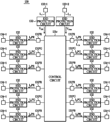
an integrated circuit (IC) substrate;
a first input pad to which a power voltage is input;
a second input pad to which a data voltage is input;
a plurality of pixel circuits configured to be mounted on the IC substrate and output the drive currents to be supplied to the plurality of pixels, wherein each of the plurality of pixel circuits includes a plurality of sub-pixel circuits including a red sub-pixel circuit that outputs a drive current supplied to a red sub-pixel, a green sub-pixel circuit that outputs a drive current supplied to a green sub-pixel, and a blue sub-pixel circuit that outputs a drive current supplied to a blue sub-pixel;
a control circuit configured to distribute the power voltage input to the first input pad and the data voltage input to the second input pad to at least one sub-pixel circuit of the plurality of sub-pixel circuits in each of the plurality of pixel circuits;
a first electrostatic discharge (ESD) protection circuit connected between the first input pad and the control circuit through a first voltage line configured to transmit, to the control circuit, the power voltage input to the first input pad;
a second ESD protection circuit connected between the second input pad and the control circuit through a second voltage line configured to transmit, to the control circuit, the data voltage input to the second input pad;
a plurality of output pads from which the drive currents to be supplied to a plurality of sub-pixels including the red sub-pixel, the green sub-pixel and the blue sub-pixel in each of the plurality of pixels are output; and
a plurality of ESD protection circuits provided on a plurality of output lines connecting the plurality of output pads to the plurality of sub-pixel circuits in each of the plurality of pixel circuits.
|