| CPC G09G 3/2092 (2013.01) [G09G 3/20 (2013.01); G09G 2310/0286 (2013.01); G09G 2310/061 (2013.01); G09G 2310/08 (2013.01); G11C 19/28 (2013.01)] | 19 Claims |
|
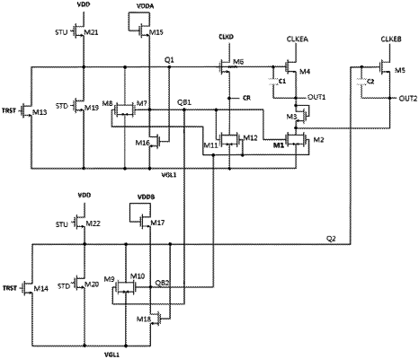
1. A shift register, wherein the shift register comprises:
a first shift register unit, wherein the first shift register unit comprises a first input circuit, a first output circuit and a first pull-down circuit, the first input circuit is connected to a first input terminal and a first pull-up node and is configured to supply a first input signal, input by the first input terminal, to the first pull-up node, the first output circuit is connected to the first pull-up node, a first output terminal and a first clock terminal and is configured to control the first output terminal to output a first output signal according to a potential of the first pull-up node and a first clock signal of the first clock terminal; and
a second shift register unit, wherein the second shift register unit comprises a second input circuit and a second output circuit, the second input circuit is connected to a second input terminal and a second pull-up node and is configured to supply a second input signal, input by the second input terminal, to the second pull-up node, the second output circuit is connected to the second pull-up node, a second output terminal and a second clock terminal and is configured to control the second output terminal to output a second output signal according to a potential of the second pull-up node and a second clock signal of the second clock terminal;
the first shift register unit further comprises a first control circuit, wherein the first control circuit is connected to the first pull-up node, a first pull-down node, a first power signal terminal and a first reference signal terminal, and the first control circuit is configured to control a potential of the first pull-down node based on a potential of the first power signal terminal and a potential of the first reference signal terminal under the control of the first pull-up node;
the second shift register unit further comprises a second control circuit, wherein the second control circuit is connected to the second pull-up node, a second pull-down node, a second power signal terminal and the first reference signal terminal, and the second control circuit is configured to control a potential of the second pull-down node based on a potential of the second power terminal and the potential of the first reference signal terminal under the control of the second pull-up node;
wherein, the first pull-down circuit is connected to the first pull-down node and the second pull-down node;
the first input circuit is connected to a fourth power source, and the first input circuit is configured to write a potential provided by the fourth power source into the first pull-up node under the control of the first input terminal; and
the second input circuit is connected to the fourth power source, and the second input circuit is configured to write the potential provided by the fourth power source into the second pull-up node under the control of the second input terminal;
wherein the first shift register unit further comprises a first reset circuit, and the first reset circuit is connected to the first pull-up node, the first reference signal terminal and a first reset terminal, and the first reset circuit is configured to reset the first pull-up node to the potential of the first reference signal terminal under the control of the first reset terminal; and
the second shift register unit further comprises a second reset circuit, and the second reset circuit is connected to the second pull-up node, the first reference signal terminal and a second reset terminal, and the second reset circuit is configured to reset the second pull-up node to the potential of the first reference signal under the control of the second reset terminal.
|