| CPC G09G 3/2003 (2013.01) [G09G 2320/0233 (2013.01); G09G 2320/0242 (2013.01)] | 13 Claims |
|
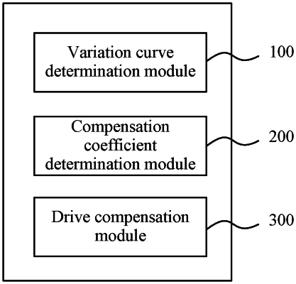
1. A drive compensation method of a display panel, wherein the display panel comprises:
a plurality of pixel units sequentially arranged in a row direction and a column direction respectively; and a plurality of signal lines extending in the row direction and the column direction respectively;
wherein the plurality of pixel units comprise first pixel units sequentially arranged in the row direction, and the plurality of signal lines comprise first signal lines extending in the column direction; and
wherein the drive compensation method comprises:
determining an impedance and capacitive reactance variation curve of one of the first signal lines in the column direction and determining a charge rate variation curve of the first pixel units in the row direction;
determining a compensation coefficient for a respective pixel unit of the plurality of pixel units in at least one of the column direction and the row direction according to the impedance and capacitive reactance variation curve of the one first signal line in at least one of the column direction and the charge rate variation curve of the first pixel units in the row direction; and
compensating the compensation coefficient for the respective pixel unit in at least one of the column direction and the row direction to a drive signal of the respective pixel unit to drive the respective pixel unit,
wherein determining the impedance and capacitive reactive variation curve of the one first signal line in the column direction comprises:
acquiring impedance and capacitive reactance of at least part of first nodes on the one first signal line, wherein one of the first pixel units is electrically connected to the one first signal line through a respective one first node of the first nodes on the one first signal line;
forming the impedance and capacitive reactance variation curve of the one first signal line in the column direction by fitting according to the impedance and capacitive reactance of the at least part of the first nodes on the one first signal line;
wherein determining the charge rate variation curve of the first pixel unit in the row direction comprises:
acquiring charge rates of at least part of the first pixel units sequentially arranged in the row direction; and
forming the charge rate variation curve of the first pixel units in the row direction by fitting according to the charge rates of the at least part of the first pixel units sequentially arranged in the row direction;
or,
wherein each pixel unit of the plurality of pixel units comprise a plurality of sub-pixels of different colors; and the determining the impedance and capacitive reactance variation curve of the one first signal line in the column direction comprises:
determining the impedance and capacitive reactance variation curve of the one first signal line in the column direction electrically connected to a plurality of sub-pixels of a same color sequentially arranged in the column direction;
wherein the determining the charge rate variation curve of the first pixel units in the row direction comprises:
determining a charge rate variation curve in the row direction of each of the plurality of sub-pixels of a same color sequentially arranged in the row direction;
wherein determining the compensation coefficients for the respective pixel unit in at least one of the column direction and the row direction according to the impedance and capacitive reactance variation curve of the one first signal line in at least one of the column direction and the change rate variation curve of the first pixel units in the row direction comprises:
determining compensation coefficients for the plurality of sub-pixels in the column direction and/or the row direction according to the impedance and capacitive reactance variation curve of the one first signal line in the column direction electrically connected to the plurality of sub-pixels of the same color sequentially arranged in the column direction and/or the charge rate variation curve in the row direction of the each sub-pixel of the same color sequentially arranged in the row direction; and
compensating the compensation coefficient for the respective pixel unit in the column direction and/or the row direction to the drive signal of the respective pixel unit to drive the respective pixel unit comprises:
compensating a compensation coefficients for a respective sub-pixel in the column direction and/or the row direction to a drive signal of the respective sub-pixel to drive the respective sub-pixel;
or,
wherein the determining the impedance and capacitive reactance variation curve of the one first signal line in at least one of the column direction and determining the charge rate variation curve of the first pixel units in the row direction comprises:
sequentially determining the impedance and capacitive reactance variation curve of the one first signal line in the column direction in each color and each gray level display state of the display panel and/or sequentially determining the charge rate variation curve of the first pixel units in the row direction in the each color and each gray level display state of the display panel,
wherein the determining the compensation coefficient for the respective pixel unit in at least one of the column direction and the row direction according to the impedance and capacitive reactance variation curve of the one first signal line in the column direction and/or the charge rate variation curve of the first pixel units in the row direction comprises:
determining compensation coefficients for the each pixel unit in the column direction and/or the row direction in the each color and each gray level display state of the display panel according to the impedance and capacitive reactance variation curve of the one first signal line in the column direction in the each color and each gray level display state of the display panel and/or the charge rate variation curve of the first pixel units in the row direction in the each color and each gray level display state of the display panel; and
wherein the compensating the compensation coefficients for the respective pixel unit in at least one of the column direction and the row direction to the drive signal of the respective pixel unit to drive the respective pixel unit comprises:
compensating the compensation coefficients corresponding to the each sub-pixel in the column direction and/or the row direction to the drive signal of the respective pixel unit according to a target emitted color and a target gray level of the pixel unit to drive the respective pixel unit.
|