| CPC G09G 3/006 (2013.01) [G09G 3/20 (2013.01); G11C 19/28 (2013.01); G09G 2310/0286 (2013.01); G09G 2310/08 (2013.01); G09G 2330/08 (2013.01); G09G 2330/12 (2013.01)] | 18 Claims |
|
1. A display apparatus, comprising:
a plurality of sub-pixels, wherein the sub-pixels are used for light-emitting display;
a plurality of signal lines, wherein the plurality of signal lines are electrically connected to the plurality of sub-pixels, respectively, and the plurality of signal lines provide signals for light-emitting display to the plurality of sub-pixels;
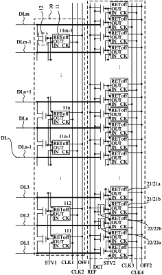
a signal line repair circuit, wherein the signal line repair circuit is electrically connected to the plurality of signal lines, and configured to repair a disconnected signal line; and
a non-display area that includes a signal line defect detection circuit;
wherein the signal line repair circuit comprises:
a plurality of connection switches, wherein an input end of each connection switch is electrically connected to one signal line, and an output end thereof is electrically connected to another signal line;
a plurality of first shift circuits, wherein the plurality of first shift circuits are sequentially cascaded, and the plurality of first shift circuits are disposed in a one-to-one correspondence with the plurality of connection switches, wherein a shift output end of each first shift unit is electrically connected to a control end of a corresponding connection switch; and
a drive chip, wherein the drive chip is electrically connected to the plurality of signal lines and the signal line repair circuit, and is configured to:
provide the signal for controlling the light-emitting display of the sub-pixels to the signal lines,
send, in response to determining that a disconnected signal line exists, a control signal to the signal line repair circuit to enable shift output ends of the plurality of first shift circuits to sequentially output enable signals, and
enable the first shift circuit corresponding to a connection switch electrically connected to the disconnected signal line to continuously output enable signals, to control the connection switch electrically connected to the disconnected signal line to be continuously turned on, so that the disconnected signal line is electrically connected to another signal line;
wherein the signal line defect detection circuit is electrically connected to the signal lines and configured to detect a defect of the signal lines, and the signal line defect detection circuit comprises:
a detection line, configured to transmit signals on the signal lines to the drive chip;
a reset line, configured to obtain a reset signal from the drive chip and transmit the reset signal to the detection line;
a plurality of detection switches, wherein the plurality of detection switches are disposed in a one-to-one correspondence with the plurality of signal lines, an input end of each detection switch is electrically connected to one signal line, an output end thereof is electrically connected to the detection line, and in response to the detection switch being turned on, a signal on the signal line electrically connected to the input end of the detection switch is transmitted to the detection line electrically connected to the output end of the detection switch; and
reset switches, wherein an input end of each reset switch is electrically connected to the repair line, and an output end thereof is electrically connected to the detection line, and wherein in response to the reset switch being turned on, a reset signal transmitted on the reset line electrically connected to the input end of the reset switch is transmitted to the detection line.
|