| CPC G09G 3/006 (2013.01) [G09G 3/20 (2013.01); G09G 2310/0275 (2013.01); G09G 2330/12 (2013.01)] | 17 Claims |
|
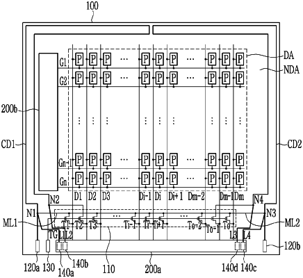
1. A display device, comprising:
a substrate comprising a display area and a non-display area disposed near the display area;
a plurality of pixels disposed in the display area;
a plurality of signal lines disposed on the substrate and connected to the pixels; and
a pad portion disposed in the non-display area and comprising a plurality of pads,
wherein the signal lines comprise:
a first crack detecting line disposed in the non-display area and directly electrically connected to a first test voltage pad and a first pad at a first node, directly electrically connected to a second pad at a second node, and extending directly across from at least a majority of one side of the display area between the first node and the second node; and
a first data line comprising a first end connected to a first transistor connected to the first crack detecting line at the second node, and a second end connected to corresponding pixels from among the plurality of pixels.
|