| CPC G06F 30/398 (2020.01) [G06F 2119/18 (2020.01)] | 20 Claims |
|
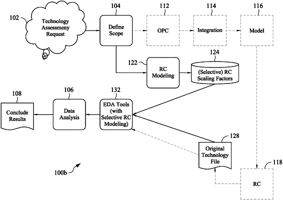
1. A method of process technology assessment, comprising:
defining a scope of the process technology assessment by assessing changes between an original process technology that includes original layout parameters and a first process technology that includes first layout parameters;
modeling a first object in an integrated circuit into a first resistance in the first process technology and a first capacitance in the first process technology;
generating a first resistance scaling factor that is multiplied by an original resistance in the original process technology to provide the first resistance and a first capacitance scaling factor that is multiplied by an original capacitance in the original process technology to provide the first capacitance;
inputting the first resistance scaling factor and the first capacitance scaling factor into an electronic design automation (EDA) tool;
inputting an original technology file corresponding to the original process technology into the EDA tool; and
utilizing, by the EDA tool, the first resistance scaling factor, the first capacitance scaling factor, and the original technology file for the simulation of the integrated circuit.
|