| CPC G06F 30/394 (2020.01) [G06F 30/392 (2020.01); H05K 3/0005 (2013.01); G06F 2113/18 (2020.01); G06F 2115/12 (2020.01); H05K 2201/09227 (2013.01)] | 20 Claims |
|
1. A pin line-out design method for a chip, applied to a ball grid array (BGA) packaged chip, the method comprising:
according to pin position information and pin definition information of the chip, determining a number of circuit board layers required for pin line-out of the chip;
allocating respective line-out layer for pins of the chip in a circuit board;
determining a pin density of the chip according to a pin spacing of the chip, and determining a specification of a via hole in the circuit board for leading the pins of the chip out to the corresponding line-out layer according to the pin density and transmission line width requirement of the chip, to perform a corresponding line-out design on the basis of the via hole;
wherein according to the pin position information and the pin definition information of the chip, determining the number of circuit board layers required for the pin line-out of the chip comprises:
determining the pin position information and the pin definition information of the chip based on a pin map of the chip, wherein the pins of the chip comprise power supply pins, low-speed pins, high-speed pins and ground pins, with a signal transmission rate on a high-speed line connected to the high-speed pins >a preset rate threshold >a signal transmission rate on a low-speed line connected to the low-speed pins;
according to the pin position information and the pin definition information, determining power supply types corresponding to the power supply pins in different positions, position information of the low-speed pins, high-speed pin pairs composed of high-speed pins in different positions, and position information of a TX pin and a RX pin in each high-speed pin pair;
determining the number of circuit board layers required for the pin line-out of the chip according to the power supply types corresponding to the power pins in different positions, the position information of all low-speed pins, and the position information of the TX pin and the RX pin in each high-speed pin pair, wherein the TX pin is a transmit pin and the RX pin is a receive pin;
wherein determining the number of circuit board layers required for the pin line-out of the chip according to the power supply types corresponding to the power pins in different positions, the position information of all low-speed pins, and the position information of the TX pin and the RX pin in each high-speed pin pair comprises:
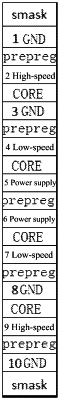
determining a flow area required by the power supply pins of a same power supply type, and determining a number of first line-out layers required by all power supply pins according to the flow area and a single-layer area of the circuit board, wherein the power supply pins of the same power supply type share one line-out layer;
determining a total number of low-speed pins according to the position information of all low-speed pins, and determining a number of second line-out layers required by all low-speed pins according to the total number of low-speed pins;
according to the position information of the TX pin and the RX pin in each high-speed pin pair, determining a number of high-speed pin pairs in a same row on the pin map, and multiplying the determined number by 2 to obtain a number of third line-out layers required by all high-speed pins, wherein the TX pin and the RX pin in each high-speed pair correspond to different line-out layers; and
adding the number of first line-out layers, the number of second line-out layers and the number of third line-out layers, and multiplying a sum of the number of first line-out layers, the number of second line-out layers and the number of third line-out layers by 2 to obtain the number of circuit board layers required for the pin line-out of the chip.
|