| CPC G06F 30/392 (2020.01) [G02B 27/0012 (2013.01); G05B 19/188 (2013.01); G06F 30/39 (2020.01); G06F 30/394 (2020.01); G06F 30/398 (2020.01); G02B 6/1228 (2013.01); G02B 6/124 (2013.01); G05B 2219/45026 (2013.01)] | 20 Claims |
|
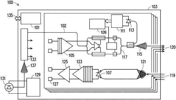
1. A method for generating a physical layout for a grating coupler integrated in a photonically-enabled circuit comprising:
receiving a photonically-enabled integrated circuit design;
receiving a parametrized wavelength of an optical beam, a parametrized first refractive index of the grating coupler, and a parametrized second refractive index of a cladding layer;
receiving a parametrized taper length of the grating coupler, a parametrized width of the grating coupler, a parametrized grating length of the grating coupler, and a parametrized incident angle of the optical beam incident onto the grating coupler;
generating a connection routing layout for the grating coupler placed on the semiconductor substrate;
generating a physical layout for the grating coupler based on the received parametrized wavelength, the parametrized first refractive index, the parametrized second refractive index, the parametrized taper length, the parametrized width, the parametrized grating length, and the parametrized incident angle, wherein the generating of the physical layout is according to a predefined model; and
outputting the physical layout of the grating coupler for manufacturing under a semiconductor fabrication process.
|