| CPC G06F 3/0655 (2013.01) [G06F 3/0604 (2013.01); G06F 3/0653 (2013.01); G06F 3/0679 (2013.01)] | 13 Claims |
|
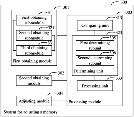
1. A method for adjusting a memory, the memory comprising a transistor, a gate of the transistor being electrically connected to a word line of the memory, one of a pair of source/drain ends of the transistor being electrically connected to a bit line of the memory via a sense amplifier and a second one of the pair of source/drain ends being electrically connected to a storage capacitor of the memory, and the method comprising:
acquiring a mapping relationship among a temperature of the transistor, a substrate bias voltage of a sense amplification transistor in the sense amplifier, and an actual data writing time of the memory;
acquiring a current temperature of the transistor; and
adjusting the substrate bias voltage on a basis of the current temperature and the mapping relationship, such that an actual data writing time corresponding to an adjusted substrate bias is within a preset writing time.
|