US 11,928,055 B2
Memory sub-system for decoding non-power-of-two addressable unit address boundaries
Patrick A. La Fratta, McKinney, TX (US); Robert Walker, Raleigh, NC (US); and Chandrasekhar Nagarajan, San Jose, CA (US)
Assigned to Micron Technology, Inc., Boise, ID (US)
Filed by Micron Technology, Inc., Boise, ID (US)
Filed on Oct. 27, 2022, as Appl. No. 17/975,164.
Application 17/975,164 is a continuation of application No. 17/204,522, filed on Mar. 17, 2021, granted, now 11,507,504.
Application 17/204,522 is a continuation of application No. 16/285,909, filed on Feb. 26, 2019, granted, now 11,016,885.
Prior Publication US 2023/0053291 A1, Feb. 16, 2023
This patent is subject to a terminal disclaimer.
Int. Cl. G06F 12/06 (2006.01); G06F 12/04 (2006.01); H04B 17/26 (2015.01); H04B 17/27 (2015.01); H04B 17/318 (2015.01); H04W 4/02 (2018.01); H04W 4/029 (2018.01); H04W 4/33 (2018.01); G06F 9/30 (2018.01); H04B 17/24 (2015.01); H04L 101/622 (2022.01); H04L 101/69 (2022.01); H04W 84/12 (2009.01)
CPC G06F 12/0607 (2013.01) [G06F 12/04 (2013.01); H04B 17/26 (2015.01); H04B 17/27 (2015.01); H04B 17/318 (2015.01); H04W 4/026 (2013.01); H04W 4/029 (2018.02); H04W 4/33 (2018.02); G06F 9/30134 (2013.01); H04B 17/24 (2015.01); H04L 2101/622 (2022.05); H04L 2101/69 (2022.05); H04W 84/12 (2013.01)] 23 Claims
OG exemplary drawing
 
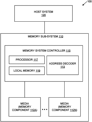
1. A system comprising:
a memory component; and
a processing device operatively coupled with the memory component, the processing device configured to perform operations comprising:
generating an internal address based on an input address, an interleaving factor, and a number of first addressable units, wherein the interleaving factor is a value that specifies a number of bytes between each channel boundary,
wherein generating the internal address comprises:
determining a lower address value, and
determining an upper address value; and
generating, using the internal address, at least a first addressable unit address.