| CPC G02F 1/1368 (2013.01) [G02F 1/136209 (2013.01); G02F 1/136222 (2021.01)] | 18 Claims |
|
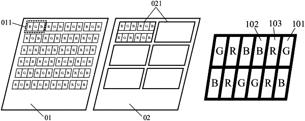
1. A display panel comprising: a display layer and a light control layer which are laminated;
wherein the light control layer comprises a plurality of light control pixel areas, the light control pixel areas comprise a thin film transistor, the display layer comprises a plurality of display pixel areas, and the display pixel areas comprise a green sub-pixel; and
an orthographic projection of the green sub-pixel on the light control pixel area is close to an area where the thin film transistor is located;
wherein the display pixel area further comprises a blue sub-pixel, and the orthographic projection of the blue sub-pixel on the light control pixel area is away from the area where the thin film transistor is located;
wherein an inside of the light control pixel area comprises a black matrix, the black matrix forming an inverted T-shape.
|