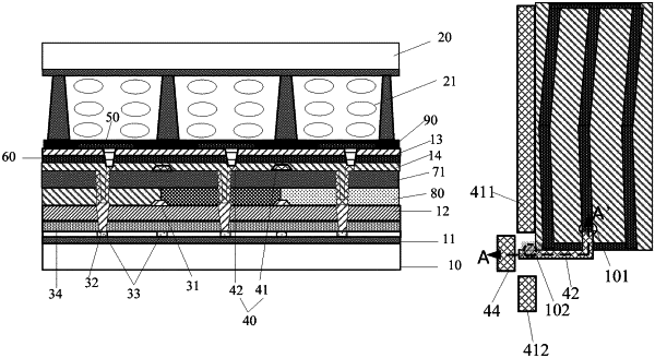
| CPC G02F 1/136286 (2013.01) [G02F 1/136209 (2013.01); G02F 1/1368 (2013.01); G06F 3/0416 (2013.01)] | 17 Claims |

|
1. A display panel, comprising:
a first substrate;
a second substrate opposite to the first substrate;
a plurality of scanning lines and a plurality of data lines located on a side of the first substrate facing the second substrate, wherein the plurality of scanning lines and the plurality of data lines cross to define a plurality of pixel regions;
a plurality of thin film transistors located on the side of the first substrate facing the second substrate, wherein the plurality of thin film transistors are in one-to-one correspondence with the plurality of pixel regions;
a first metal electrode layer located on a side of the plurality of thin film transistors facing away from the first substrate, wherein the first metal electrode layer comprises a plurality of first metal electrode lines and a plurality of second metal electrode lines; and
a pixel electrode layer and a common electrode layer located on a side of the first metal electrode layer facing away from the first substrate, wherein the pixel electrode layer comprises a plurality of pixel electrode units, the plurality of pixel electrode units are in one-to-one correspondence with the plurality of pixel regions, and the common electrode layer comprises a plurality of common electrode units,
wherein each of the plurality of first metal electrode lines is electrically connected to a respective common electrode unit of the plurality of common electrode units, to provide a common voltage signal to a common electrode unit in a first time period, and provide a touch driving signal to the common electrode unit in a second time period, wherein each of a plurality of second metal electrode line has a first end electrically connected to a drain of the thin film transistor, and a second end electrically connected to the pixel electrode unit,
wherein each of the plurality of second metal electrode line comprises a first end electrically connected to the drain of the thin film transistor through a first via hole, and a second end electrically connected to the pixel electrode unit through a second via hole,
wherein each of the plurality of first metal electrode lines comprises a first part parallel to an extension direction of the data line of the plurality of data lines and a second part parallel to the extension direction of the data line of the plurality of data lines;
the projection of the second via hole on the first substrate is located between a projection of a first portion on the first substrate and a projection of the second portion on the first substrate, and the second via hole is insulated from the first portion and the second portion; and
the first metal electrode layer further comprises a metal connecting line, and the first portion and the second portion are electrically connected by means of the metal connecting wire.
|