| CPC G02F 1/13398 (2021.01) [G02F 1/1337 (2013.01); G02F 1/137 (2013.01)] | 17 Claims |
|
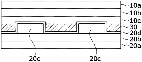
1. An optical device, comprising:
a liquid crystal element having a top surface, a bottom surface, and sides separating the top surface and the bottom surface; and
an outer layer surrounding the sides of the liquid crystal element, wherein the liquid crystal element comprises:
a first base layer;
a second base layer;
a liquid crystal layer positioned between the first base layer and the second base layer;
a pressure-sensitive adhesive layer positioned between the first base layer and the liquid crystal layer; and
a spacer to maintain a gap between the first base layer and the second base layer,
wherein the optical device satisfies Equation 1:
−T2×0.4≤T1−T2≤T2×0.4 [Equation 1]
wherein, T1 is a thickness of the outer layer, and T2 is a thickness of the liquid crystal element.
|