| CPC G02F 1/133388 (2021.01) [G02F 1/13306 (2013.01); G02F 1/133354 (2021.01); G02F 1/13452 (2013.01); G02F 1/136286 (2013.01); G02F 1/1368 (2013.01); G09G 3/3677 (2013.01); H01L 27/124 (2013.01); H01L 27/1259 (2013.01); G09G 2300/0408 (2013.01); G09G 2300/0426 (2013.01); G09G 2310/08 (2013.01); G09G 2320/043 (2013.01); G09G 2330/02 (2013.01)] | 18 Claims |
|
1. A display substrate, comprising:
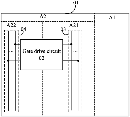
a base substrate comprising a display region and a non-display region surrounding the display region, wherein the non-display region comprises a peripheral region and an encapsulation region sequentially arranged along a direction away from the display region, a sealant being coated in the encapsulation region;
a gate drive circuit disposed in the non-display region;
a plurality of first signal lines disposed in the peripheral region and connected to the gate drive circuit;
a plurality of second signal lines disposed in the non-display region and connected to the gate drive circuit; and
a transistor device layer disposed on the base substrate, wherein the transistor device layer is configured to form a plurality of thin-film transistors in the gate drive circuit, and is provided with a via, wherein the via is configured to connect a gate layer to a source and drain layer in the transistor device layer;
wherein each of the first signal line and the second signal line is configured to supply a signal to the gate drive circuit, and a frequency of the signal supplied by the first signal line is lower than a frequency of the signal supplied by the second signal line; and the display substrate comprises a plurality of gate drive circuits cascaded in sequence; wherein a number of the vias disposed in a region where each of the gate drive circuits is disposed is less than a number of the thin-film transistors in the gate drive circuit.
|