| CPC G02B 6/4295 (2013.01) [G02B 6/12004 (2013.01); G02B 6/4274 (2013.01); G02B 6/4283 (2013.01); G02B 6/4286 (2013.01); H01S 5/026 (2013.01); H01S 5/0264 (2013.01); H01S 5/2018 (2013.01); G02B 2006/12085 (2013.01); G02B 2006/12097 (2013.01); G02B 2006/12121 (2013.01); G02B 2006/12123 (2013.01); G02B 2006/12128 (2013.01); G02B 2006/12138 (2013.01)] | 22 Claims |
|
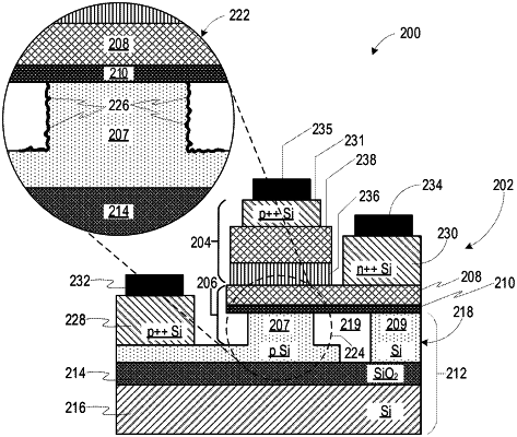
1. An optical device, comprising:
a light-emitting structure to emit light upon application of electricity to the optical device; and
a waveguide integrated capacitor formed under the light-emitting structure to monitor the light emitted by the light-emitting structure, wherein the waveguide integrated capacitor comprises a waveguide region carrying at least a portion of the light, and wherein the waveguide region comprises one or more photon absorption sites for absorbing photons of the portion of the light carried in the waveguide region and causing generation of free charge carriers relative to an intensity of the light confined in the waveguide region based on the absorbed photons resulting in a change in a conductance of the waveguide region that is proportional to the intensity of the portion of the light carried in the waveguide region.
|