| CPC G01R 31/31722 (2013.01) [G01R 31/31723 (2013.01); G01R 31/31724 (2013.01); G01R 31/31725 (2013.01); H01L 22/34 (2013.01)] | 20 Claims |
|
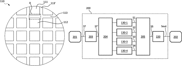
1. A semiconductor wafer, comprising:
a scribe line between a first row of dies and a second row of dies; and
a first conductive contact and a second conductive contact disposed on the scribe line;
a benchmark circuit disposed on the scribe line and electrically coupled to the first conductive contact and the second conductive contact, the benchmark circuit comprising:
a first device-under-test (DUT);
a second DUT;
a first switching circuit configured to selectively couple the first DUT and the second DUT to the first conductive contact; and
a second switching circuit configured to selectively couple the first DUT and the second DUT to the second conductive contact.
|