| CPC G01R 31/2831 (2013.01) [G06F 16/21 (2019.01); G06F 30/36 (2020.01); H01L 22/00 (2013.01)] | 20 Claims |
|
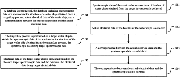
1. A method for simulating electricity of a wafer chip, comprising:
constructing a database, the database comprising spectroscopic data of a semiconductor structure of the wafer chip obtained from a target key process, actual electrical data of the wafer chip, and a correspondence between the spectroscopic data and the actual electrical data,
performing the target key process on a target wafer chip to obtain the spectroscopic data of the semiconductor structure of the target wafer chip obtained from the target key process, the spectroscopic data being target spectroscopic data; and
simulating electrical data of the target wafer chip based on the obtained target spectroscopic data and the database, the electrical data being target electrical data.
|