| CPC G01R 1/07342 (2013.01) [G01R 1/0491 (2013.01); G01R 33/072 (2013.01)] | 22 Claims |
|
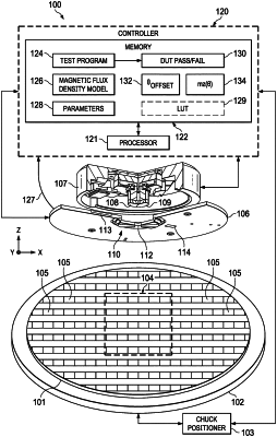
1. A method of manufacturing an electronic device, the method comprising:
initializing a wafer probe test system to test a wafer that is positioned in a wafer plane of orthogonal first and second directions, including:
measuring a probe needle height along a third direction that is orthogonal to the first and second directions, and
using a magnetic sensor of the wafer probe test system, measuring a magnetic field of a rotary magnet rotating about an axis along the third direction at different rotational angles; and
while the rotary magnet rotates, testing magnetic sensing performance of circuits of respective test sites of the wafer according to a model of magnetic flux density in the first, second and third directions at the respective test sites of the wafer as a function of the rotational angle of the rotary magnet, the probe needle height and measured magnetic flux density of the magnetic sensor.
|