| CPC B29D 11/0073 (2013.01) [B32B 7/023 (2019.01); B32B 7/12 (2013.01); B32B 17/10 (2013.01); B32B 2307/412 (2013.01); B32B 2307/418 (2013.01); B32B 2551/00 (2013.01); G02B 6/136 (2013.01)] | 17 Claims |
|
1. A method for manufacturing an optical element, and the method comprising:
providing a carrier;
attaching a bonding layer to a surface of the carrier;
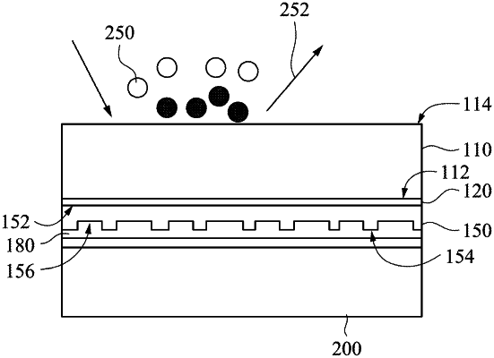
forming a mold layer on the bonding layer, wherein the mold layer has a first surface and a second surface, which are opposite to each other, the first surface is adjacent to the bonding layer, and the second surface is set with a plurality of microstructures;
performing an anti-sticking treatment on the second surface of the mold layer;
forming an optical layer on the second surface of the mold layer after performing the anti-sticking treatment, wherein the optical layer covers and fills the microstructures;
adhering a transparent substrate to the optical layer using an adhesive layer, wherein the optical layer and the transparent substrate are respectively located on two opposite sides of the adhesive layer;
removing the carrier from the bonding layer; and
removing the bonding layer and the mold layer from the optical layer.
|