| CPC H10N 50/80 (2023.02) [G11C 11/161 (2013.01); H01F 10/3286 (2013.01); H01F 41/307 (2013.01); H10B 61/00 (2023.02); H10N 50/01 (2023.02); H10N 50/10 (2023.02); H01F 10/3272 (2013.01); H01F 10/329 (2013.01)] | 18 Claims |

|
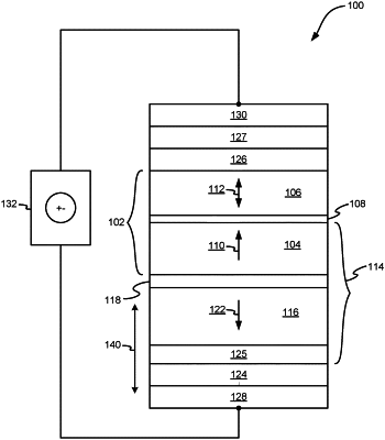
1. A magnetic random access memory element, comprising:
a magnetic reference layer;
a magnetic free layer;
a non-magnetic barrier layer disposed below the magnetic free layer and above the magnetic reference layer; and
a MgO layer contacting the magnetic free layer and being disposed adjacent the magnetic free layer, the magnetic free layer being formed between the non-magnetic barrier layer and the MgO layer, the MgO layer comprising multiple homogeneous layers of MgO and having an area resistance of less than 1.5 Ωμm2 and being negligible compared to an area resistance of the non-magnetic barrier layer.
|