| CPC H10K 65/00 (2023.02) [H10K 39/32 (2023.02); H10K 50/16 (2023.02); H10K 50/17 (2023.02); H10K 50/865 (2023.02); H10K 59/12 (2023.02); H10K 59/40 (2023.02); H10K 2101/30 (2023.02)] | 11 Claims |

|
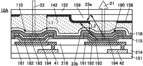
1. A display unit comprising:
a light-receiving device comprising:
a first pixel electrode;
an active layer over the first pixel electrode; and
a common electrode over the active layer;
a light-emitting device comprising:
a second pixel electrode;
a light-emitting layer over the second pixel electrode;
an electron-transport layer over the light-emitting layer; and
the common electrode over the electron-transport layer;
a light-blocking layer over the common electrode;
a resin layer over the light-blocking layer; and
a substrate over the resin layer,
wherein a first part of the light-blocking layer and a part of the resin layer overlap each other,
wherein a second part of the light-blocking layer and the resin layer do not overlap each other,
wherein a shortest distance between the common electrode and the first part of the light-blocking layer is smaller than a shortest distance between the common electrode and the second part of the light-blocking layer,
wherein the electron-transport layer comprises a first region and a second region,
wherein each of the first region and the second region comprises an electron-transport material and a first substance,
wherein the first region has a different concentration of the first substance from the second region, and
wherein the first substance is one of a metal, a metallic salt, a metal oxide and an organometallic complex.
|