| CPC H10K 59/131 (2023.02) [G09G 3/3208 (2013.01); G09G 3/3233 (2013.01); G09G 3/3266 (2013.01); G09G 3/3275 (2013.01); H01L 27/124 (2013.01); H05K 1/189 (2013.01); H10K 50/81 (2023.02); H10K 50/82 (2023.02); H10K 50/8426 (2023.02); H05K 2201/10128 (2013.01)] | 14 Claims |

|
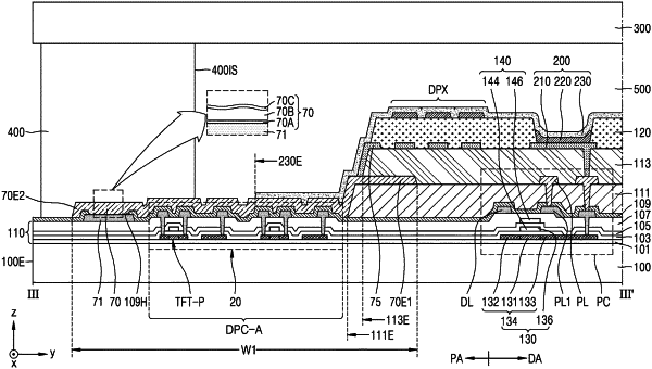
1. A display device, comprising:
a substrate;
an encapsulation substrate on the substrate;
a sealing material interposed between the substrate and the encapsulation substrate;
a light-emitting diode in a display area of the substrate and comprising a first electrode, and a second electrode on the first electrode, and an intermediate layer between the first electrode and the second electrode;
an inorganic insulating layer on the substrate and being disposed under the sealing material;
a first organic insulating layer disposed on the inorganic insulating layer, the first organic insulating layer being interposed between the light-emitting diode and the inorganic insulating layer and not being disposed under the sealing material;
a power supply line on the inorganic insulating layer, the power supply line being in the peripheral area surrounding the display area; and
a conductive layer, wherein the power supply line, the conductive layer, and the second electrode of the light-emitting diode are electrically connected to each other;
wherein apart of the conductive layer overlaps the power supply line, and a part of the second electrode of the light-emitting diode overlaps the conductive layer,
wherein the sealing material comprises an inner surface facing the display area and an outer surface opposite to the inner surface, and a first distance from the outer surface of the sealing material to an edge of the power supply line is less than a second distance from the outer surface of the sealing material to an edge of the second electrode of the light-emitting diode, and
wherein the power supply line extends past the inner surface of the sealing material and is disposed above the first organic insulating layer such that the first organic insulating layer is disposed between the power supply line and the inorganic insulating layer.
|