| CPC H10K 59/126 (2023.02) [H01L 27/124 (2013.01); H10K 59/1213 (2023.02); H10K 59/1216 (2023.02); H10K 59/131 (2023.02); G02F 1/136213 (2013.01); G02F 1/136218 (2021.01); G02F 1/13629 (2021.01)] | 15 Claims |

|
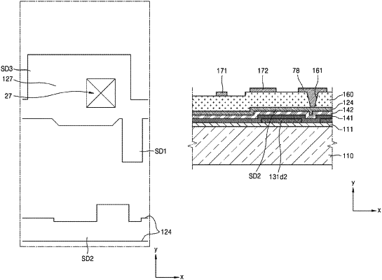
1. A display apparatus comprising:
a first thin-film transistor comprising a first gate electrode and a first semiconductor layer;
a first electrode layer overlapping the first gate electrode;
a first voltage line extended in a first direction and electrically connected to the first electrode layer;
a data line extended in the first direction; and
a second thin-film transistor comprising a second gate electrode and a second semiconductor layer, the second semiconductor layer being extended from one end of the first semiconductor layer and being electrically connected to the data line; and
wherein the first semiconductor layer is extended in a second direction perpendicular to the first direction and the second semiconductor layer is extended in the first direction,
wherein the first electrode layer overlaps the first semiconductor layer and the second semiconductor layer, in a plan view, and
wherein a length along the first direction of the overlapping part of the first electrode layer with the second semiconductor layer is longer than a length along the first direction of the first gate electrode.
|