| CPC H10K 59/122 (2023.02) [H10K 50/844 (2023.02); H10K 59/40 (2023.02); H10K 50/15 (2023.02); H10K 50/16 (2023.02); H10K 50/17 (2023.02); H10K 50/171 (2023.02); H10K 50/816 (2023.02); H10K 50/828 (2023.02); H10K 50/8426 (2023.02)] | 20 Claims |

|
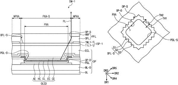
1. A display apparatus comprising:
a display panel comprising:
a first electrode;
a pixel defining layer comprising a first opening that exposes at least a portion of the first electrode;
a light emitting layer disposed on the first electrode;
a display device layer comprising a second electrode disposed on the light emitting layer; and
a thin-film encapsulation layer that overlaps the display device layer;
an input sensing panel disposed on the thin-film encapsulation layer and comprising a sensing insulation layer and a conductive layer; and
an organic insulation layer that overlaps the sensing insulation layer and comprises a second opening overlapping the first opening, wherein
a side surface of the organic insulation layer defines the second opening and comprises protruding side surfaces inclined in different directions as compared to a side surface of the pixel defining layer in plan view, and
the side surface of the pixel defining layer defines the first opening.
|