| CPC H10K 59/1213 (2023.02) [H01L 27/1244 (2013.01); H10K 59/1216 (2023.02); H10K 59/123 (2023.02); H10K 59/124 (2023.02); H10K 59/126 (2023.02); H10K 59/131 (2023.02); H10K 77/111 (2023.02); H01L 27/1225 (2013.01); H01L 27/1251 (2013.01); H01L 27/1255 (2013.01); H01L 27/1274 (2013.01); H01L 27/1288 (2013.01); H01L 29/78633 (2013.01); H01L 29/78675 (2013.01); H01L 29/7869 (2013.01); H10K 59/1201 (2023.02); H10K 59/353 (2023.02); H10K 2102/311 (2023.02); H10K 2102/341 (2023.02)] | 20 Claims |

|
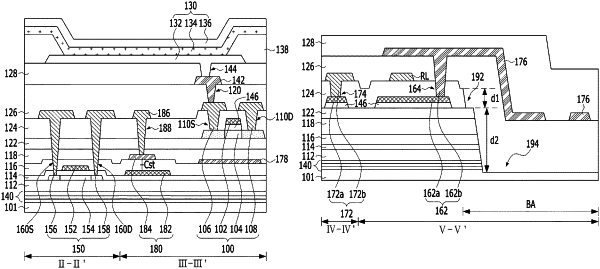
1. A display device comprising:
a substrate including an active area and a bending area;
a first thin film transistor on the active area of the substrate, the first thin film transistor including a first semiconductor layer;
a second thin film transistor spaced away from the first thin film transistor in the active area of the substrate, the second thin film transistor including a second semiconductor layer;
an upper interlayer dielectric film on the first semiconductor layer and the second semiconductor layer;
a first planarization layer on the upper interlayer dielectric film, the first planarization layer extending to the bending area of the substrate;
a pixel connection electrode on the first planarization layer in active area, the pixel connection electrode electrically connected to the second thin film transistor;
a second planarization layer on the first planarization layer, the second planarization layer covering the pixel connection electrode;
an organic light-emitting device including an anode electrode connected to the pixel connection electrode, a light-emitting stack on the anode electrode, and a cathode electrode on the light-emitting stack; and
a signal link between the first planarization layer and the second planarization layer in the bending area, the signal link including a same material as the pixel connection electrode,
wherein a distance between the substrate and the signal link in the bending area is smaller than a distance between the substrate and the pixel connection electrode on the active area.
|