| CPC H10K 50/844 (2023.02) [H10K 59/131 (2023.02); H01L 27/1222 (2013.01); H01L 27/124 (2013.01); H01L 27/1248 (2013.01); H01L 29/78675 (2013.01); H01L 29/78678 (2013.01); H10K 50/84 (2023.02); H10K 59/1201 (2023.02); H10K 59/122 (2023.02); H10K 59/124 (2023.02); H10K 2102/351 (2023.02)] | 20 Claims |

|
1. An organic light-emitting diode (OLED) display, comprising:
a substrate comprising a display area and a non-display area, wherein the substrate extends in a first direction and a second direction that crosses the first direction;
a buffer layer on the substrate;
a plurality of thin film transistors (TFT) on the buffer layer, the thin film transistor comprising an active layer, a gate electrode, a source electrode and a drain electrode;
a plurality of OLEDs that include a plurality of light emitting layers between a plurality of lower electrodes and an upper electrode on the substrate;
a thin film encapsulation layer on the upper electrode;
a dam disposed in the non-display area and surrounds the display area;
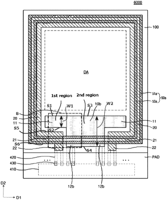
a first voltage line disposed in the non-display area, wherein the first voltage line includes a first region and a second region arranged along the first direction; and
a second voltage line disposed in the non-display area, wherein the second voltage line extends in the first direction adjacent to the first region, but does not extend in the first direction adjacent to the second region,
wherein the first region and the second region each have a first width and a second width in the second direction, and the second width is greater than the first width, and wherein the dam overlaps the second region of the first voltage line in a plan view.
|