| CPC H10K 50/13 (2023.02) [H10K 50/156 (2023.02); H10K 50/157 (2023.02); H10K 50/166 (2023.02); H10K 50/171 (2023.02); H10K 50/18 (2023.02); H10K 50/805 (2023.02); H10K 59/32 (2023.02)] | 15 Claims |

|
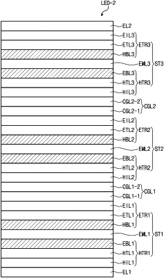
1. A light emitting device comprising:
a first electrode;
a first stack on the first electrode;
a first charge generation layer on the first stack;
a second stack on the first charge generation layer; and
a second electrode on the second stack, wherein
the first stack comprises a first light emitting layer, a first hole transport region between the first electrode and the first light emitting layer, and a first electron transport region between the first light emitting layer and the first charge generation layer,
the second stack comprises a second light emitting layer, a second hole transport region between the first charge generation layer and the second light emitting layer and a second electron transport region between the second light emitting layer and the second electrode,
the first light emitting layer and the second light emitting layer are to generate blue light,
the first hole transport region comprises a first hole injection layer, a first hole transport layer between the first hole injection layer and the first light emitting layer, and a first electron blocking layer between the first hole transport layer and the first light emitting layer,
the first electron transport region comprises a first electron injection layer, a first electron transport layer between the first electron injection layer and the first light emitting layer, and a first hole blocking layer between the first electron transport layer and the first light emitting layer,
the second hole transport region comprises a second hole injection layer, a second hole transport layer between the second hole injection layer and the second light emitting layer, and a second electron blocking layer between the second hole transport layer and the second light emitting layer,
the second electron transport region comprises a second electron injection layer, a second electron transport layer between the second electron injection layer and the second light emitting layer, and a second hole blocking layer between the second electron transport layer and the second light emitting layer,
at least one selected from the first electron blocking layer, the first hole blocking layer, the second electron blocking layer, and the second hole blocking layer comprises a light emitting material,
the light emitting material is a material to generate green light, red light, and/or orange light having a higher wavelength than that of the light generated by the first light emitting layer and the second light emitting layer, and
the at least one selected from the first electron blocking layer, the first hole blocking layer, the second electron blocking layer, and the second hole blocking layer, comprising the light emitting materials, comprises a base substance and the light emitting material doped in the base substance.
|