| CPC H10B 43/50 (2023.02) [H01L 23/5226 (2013.01); H01L 23/528 (2013.01); H10B 41/10 (2023.02); H10B 41/40 (2023.02); H10B 41/50 (2023.02); H10B 43/10 (2023.02); H10B 63/30 (2023.02); H10B 41/27 (2023.02); H10B 43/27 (2023.02)] | 16 Claims |

|
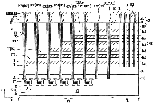
1. A semiconductor memory device comprising:
a peripheral transistor;
a first insulating layer covering the peripheral transistor;
a source layer on the first insulating layer;
a stack structure including conductive patterns on the source layer;
a peripheral contact structure penetrating the stack structure and the source layer, the peripheral contact structure being electrically connected to the peripheral transistor; and
a word line contact electrically connected to at least one of the conductive patterns,
wherein the stack structure includes a stepped structure including a step side surface and a step top surface,
wherein the peripheral contact structure is in contact with the step side surface, and
wherein the peripheral contact structure is electrically connected to the word line contact.
|