| CPC H10B 43/27 (2023.02) [G11C 5/063 (2013.01); H10B 43/35 (2023.02)] | 23 Claims |

|
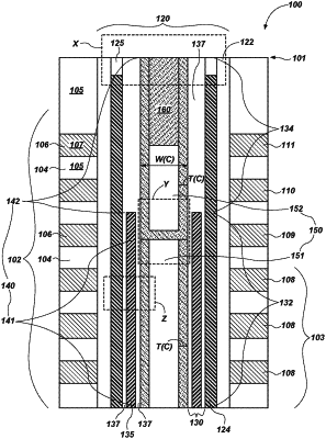
1. A microelectronic device, comprising:
a stack structure comprising insulative structures interleaved with conductive structures;
at least one select gate structure over the stack structure;
a first tunneling structure extending vertically through the stack structure, the first tunneling structure comprising a high-κ material;
a second tunneling structure extending vertically through the at least one select gate structure, the second tunneling structure being devoid of the high-κ material, an entirety of the high-κ material of the first tunneling structure being elevationally below the second tunneling structure; and
a channel structure extending vertically through the stack structure and the at least one select gate structure, the channel structure being horizontally interior to the first tunneling structure and the second tunneling structure,
the channel structure comprising:
a first channel portion; and
a second channel portion above the first channel portion,
the first channel portion differing from the second channel portion in at least one of a thickness of a semiconductor material, a horizontal outer dimension of the semiconductor material, and a composition of the semiconductor material.
|