| CPC H10B 43/27 (2023.02) [H10B 41/10 (2023.02); H10B 41/27 (2023.02); H10B 43/10 (2023.02); H10B 43/35 (2023.02)] | 20 Claims |

|
1. A vertical semiconductor device, comprising:
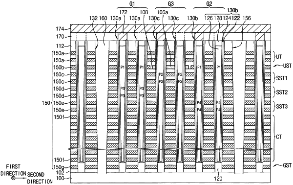
first gate patterns on a substrate, the first gate patterns being spaced apart from each other in a vertical direction perpendicular to an upper surface of the substrate, the first gate patterns as gates of a ground selection transistor and a cell transistor;
upper selection lines on the first gate patterns, wherein the upper selection lines are separated by a first trench, and at least two first trenches are disposed at the same level; and
channel structures passing through the first gate patterns and the upper selection lines, each of the channel structures extending to the upper surface of the substrate, and each of the channel structures including a charge storage structure and a channel,
wherein, in a plan view of the upper selection lines cut along a horizontal direction, one sidewall the first trench overlaps sidewalls of the channel structures.
|