| CPC H10B 12/50 (2023.02) [H01L 23/3171 (2013.01); H01L 23/3185 (2013.01); H01L 23/528 (2013.01); H01L 29/42352 (2013.01); H01L 29/4236 (2013.01); H01L 29/7827 (2013.01); H01L 29/7926 (2013.01); H10B 43/27 (2023.02); H10B 43/30 (2023.02); H10B 43/35 (2023.02); H10B 43/40 (2023.02); H10B 43/50 (2023.02); H01L 2924/0002 (2013.01)] | 15 Claims |

|
1. A vertical memory device comprising:
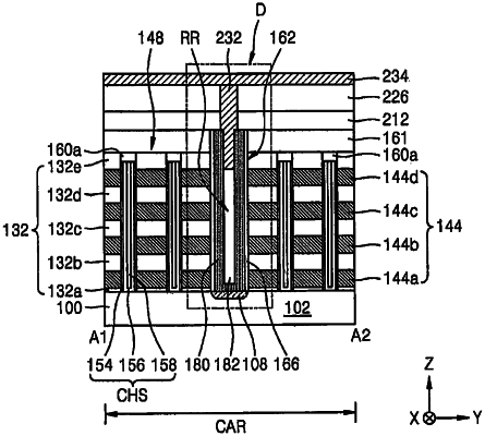
a cell gate stack structure on a substrate, the cell gate stack structure comprising a plurality of cell gate lines spaced apart from one another in a vertical direction, and an opening adjacent to the plurality of cell gate lines, the opening passing through the cell gate stack structure;
a contact plug in the opening, the contact plug comprising an inner sidewall delimiting a recessed region in the opening;
a buried film pattern in a portion of the recessed region, the buried film pattern being formed of a Si-containing material;
a contact overlying the buried film pattern, the contact comprising an inner contact portion disposed in the recessed region; and
a separation film pattern interposed between the plurality of cell gate lines and the contact plug,
wherein the contact plug comprises a conductive metal nitride, and
wherein the inner contact portion of the contact is in contact with the buried film pattern within the recessed region.
|