| CPC H05K 1/0251 (2013.01) [H05K 1/115 (2013.01); H05K 3/366 (2013.01); H05K 2201/10098 (2013.01)] | 20 Claims |

|
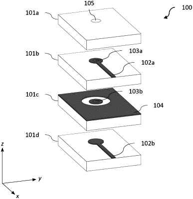
1. A substrate comprising:
a first dielectric substrate including a first face, a second face, and a first through-hole penetrating the first dielectric substrate from the first face to the second face;
a second dielectric substrate including a third face, a fourth face, and a first conductive via penetrating the second dielectric substrate from the third face to the fourth face;
a first signal line provided between the first dielectric substrate and the second dielectric substrate;
a third dielectric substrate including a fifth face, a sixth face, and a second conductive via penetrating the third dielectric substrate from the fifth face to the sixth face;
a first planar conductor provided between the second dielectric substrate and the third dielectric substrate, the first planar conductor being located away from the first conductive via and the second conductive via;
a fourth dielectric substrate; and
a second signal line provided between the third dielectric substrate and the fourth dielectric substrate,
wherein:
at least a part of a first inner wall of the first dielectric substrate at a portion where the first through-hole is provided is not covered with a conductor,
the first through-hole and the first conductive via at least partially overlap in a first direction in which at least one of the first conductive via and the second conductive via penetrate,
the first conductive via and the second conductive via at least partially overlap in the first direction, and
the second conductive via and the second signal line at least partially overlap in the first direction.
|