| CPC H05K 1/0218 (2013.01) [H05K 1/116 (2013.01); H05K 2201/09381 (2013.01); H05K 2201/0939 (2013.01)] | 20 Claims |

|
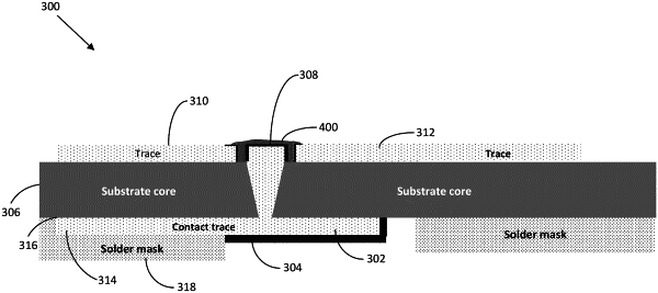
1. A printed circuit board for an electronic device, comprising:
a substrate having a first side and a second side opposite to the first side;
a contact finger disposed on the first side of the substrate configured to interface with an external electronic device;
a contact trace coupled to the contact finger and extending from the first side of the substrate to the second side of the substrate, wherein the contact trace has an exposed portion disposed on the second side of the substrate in the form of a via connection pad; and
an impedance trace disposed on the second side of the substrate and configured to be coupled to one or more components of the electronic device;
an outer pad coupled to the impedance trace, wherein the outer pad surrounds the via connection pad and is electrically separated from the via connection pad by a separation distance;
wherein the contact finger and the via connection pad are plated with a common material to reduce galvanic etching of the contact trace; and
wherein the via connection pad of the contact trace is electrically connected to the impedance trace by way of a solder joint.
|