| CPC H05K 1/0216 (2013.01) [H01P 1/365 (2013.01); H01Q 1/38 (2013.01); H01Q 1/48 (2013.01); H01Q 1/525 (2013.01); H01Q 17/00 (2013.01); H05K 1/0206 (2013.01); H05K 3/4644 (2013.01); H05K 2201/10098 (2013.01)] | 20 Claims |

|
1. An apparatus comprising:
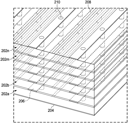
an isolation barrier configured to absorb electromagnetic energy, the isolation barrier comprising:
multiple layers stacked on one another, each of the multiple layers comprising at least one dielectric material, at least one thin-film resistive material carried by the at least one dielectric material, and conductive strips in electrical contact with the at least one thin-film resistive material; and
vias through the multiple layers, multiple ones of the vias positioned along each of the conductive strips, the vias electrically coupling the conductive strips in the multiple layers to one another;
wherein the isolation barrier is configured to guide the electromagnetic energy through the multiple layers to enable absorption of the electromagnetic energy by the at least one thin-film resistive material.
|