| CPC H04B 10/803 (2013.01) [H04B 1/04 (2013.01); H04B 10/556 (2013.01); H04B 2001/0408 (2013.01)] | 21 Claims |

|
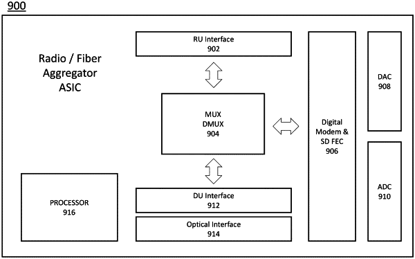
1. A CMOS integrated circuit comprising:
digital-to-analogue converters (DACs);
analogue-to-digital converters (ADCs);
a digital signal processor (DSP);
on-chip switching;
an on-chip processor; and
logic enabling the CMOS integrated circuit to:
receive data from a plurality of data sources in a 5G network;
combine the data from the plurality of data sources into a single data stream;
encode the single data stream using the DSP; and
cause the encoded single data stream to be transmitted to another device in the 5G network,
wherein the transmission is over a transmission medium, and
wherein the transmission medium is chosen from the group consisting of an optical link, a mm Wave link, a radio link, and a SERDES link.
|