| CPC H03L 7/0807 (2013.01) [H03L 7/0816 (2013.01); H03L 7/0994 (2013.01)] | 16 Claims |

|
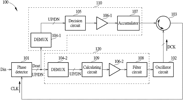
1. A clock data recovery circuit, comprising:
a phase detector, configured to receive an input data signal and a plurality of first clock signals and sample the input data signal according to the first clock signals to generate an up control signal and a down control signal;
a first signal processing path, coupled to the phase detector and comprising at least one first signal processing device configured to receive the up control signal and the down control signal and generate a phase control signal according to the up control signal and the down control signal;
a second signal processing path, coupled to the phase detector and comprising at least one second signal processing device configured to receive the up control signal and the down control signal and generate a frequency control signal according to the up control signal and the down control signal;
an oscillator circuit, configured to generate a plurality of second clock signals according to the frequency control signal; and
a phase control circuit, configured to receive the second clock signals and the phase control signal and control phases of the second clock signals according to the phase control signal to generate the first clock signals.
|