| CPC H03K 3/012 (2013.01) [H03K 17/56 (2013.01)] | 20 Claims |

|
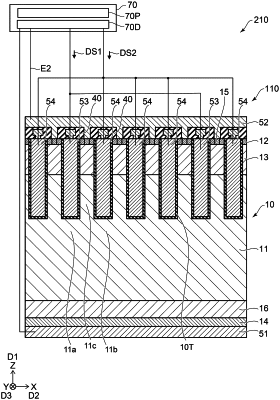
1. A drive device, comprising:
a drive circuit configured to drive a semiconductor device,
the semiconductor device including
a first electrode,
a semiconductor member including
a first semiconductor region of a first conductive type,
a second semiconductor region of the first conductive type,
a third semiconductor region of a second conductive type, and
a fourth semiconductor region of the second conductive type,
the first semiconductor region including a first partial region, a second partial region, and a third partial region,
the first semiconductor region being located between the first electrode and the second semiconductor region in a first direction,
the third semiconductor region being located between the first semiconductor region and the second semiconductor region in the first direction,
the fourth semiconductor region being located between the first electrode and the first semiconductor region in the first direction;
a second electrode electrically connected to the second semiconductor region,
a third electrode, the first partial region being located between the fourth semiconductor region and the third electrode in the first direction,
a fourth electrode, a second direction from the third electrode to the fourth electrode crossing the first direction, the second partial region being located between the fourth semiconductor region and the fourth electrode in the first direction, at least a part of the third partial region being located between the third electrode and the fourth electrode, at least a part of the second semiconductor region and at least a part of the third semiconductor region being located between the third electrode and the fourth electrode in the second direction, and
an insulating member, at least a part of the insulating member being provided between the semiconductor member and the third electrode, and between the semiconductor member and the fourth electrode,
the drive circuit being configured to supply a first drive signal to the third electrode and to supply a second drive signal to the fourth electrode,
in a first operation, the first drive signal being configured to change from a first potential to a second potential higher than the first potential, and
in the first operation, the second drive signal being configured to change from a third potential to a fourth potential higher than the third potential, and to change to a fifth potential between the third potential and the fourth potential after the changing from the third potential to the fourth potential,
wherein an absolute value of a difference between the third potential and the fifth potential is not less than 0.3 times and not more than 0.7 an absolute value of a difference between the third potential and the fourth potential.
|