| CPC H03K 19/0005 (2013.01) [G11C 16/0483 (2013.01)] | 18 Claims |

|
1. A semiconductor device comprising:
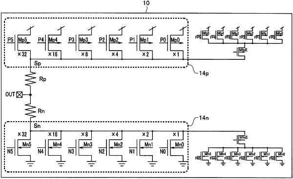
a buffer configured to perform data transmission by turning on and off a first output transistor group and a second output transistor group;
a first correction circuit including the first output transistor group and configured to calibrate a resistance value of the buffer by controlling on-off state of each of first transistors of the first output transistor group, wherein each of the first transistors is set to a resistance value with a different weight;
a second correction circuit including the second output transistor group and configured to calibrate the resistance value of the buffer by controlling an on-off state of each of second transistors of the second output transistor group, wherein each of the second transistors is set to a resistance value equal to or smaller than the resistance value of a transistor with a lightest weight among the first transistors; and
a control circuit configured to:
cause the calibration by the first correction circuit to be performed in a non-communication duration other than a duration of data transmission from the buffer;
control to start the data transmission from the buffer; and
cause the calibration by the second correction circuit to be performed in at least the duration of the data transmission from the buffer after a duration of the calibration by the first correction circuit,
wherein the first output transistor group has a first variable resistance value and the second output transistor group has a second variable resistance value that is equal to or less than the first variable resistance value.
|