| CPC H03K 17/6872 (2013.01) [G06F 1/28 (2013.01); H03K 19/018571 (2013.01)] | 20 Claims |

|
1. A circuit, comprising:
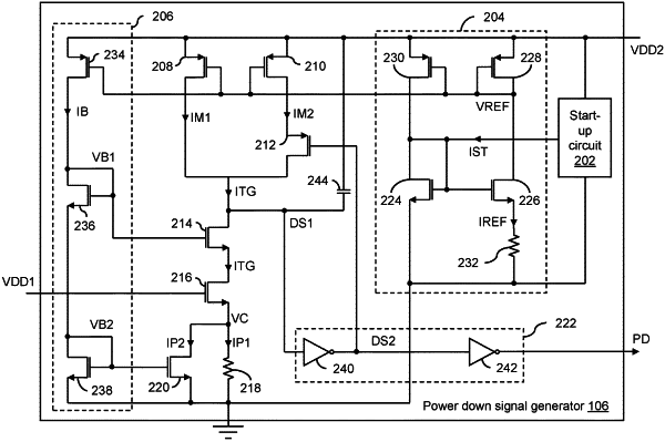
a power down signal generator configured to generate a power down signal, the power down signal generator comprising:
a detection transistor configured to receive (i) a first supply voltage in a first voltage domain and (ii) a target current;
a first resistor coupled in series with the detection transistor, wherein the first resistor has a control voltage generated thereacross based on a first part of the target current; and
a compensation transistor that is coupled in parallel to the first resistor, and configured to (i) receive a first bias voltage that is derived from a second supply voltage in a second voltage domain and (ii) sink, based on the first bias voltage, a second part of the target current to maintain the control voltage within a first predefined range,
wherein an operational state of the detection transistor is controlled based on the first supply voltage and the control voltage, and
wherein the generation of the power down signal is controlled based on the operational state of the detection transistor.
|