| CPC H03K 17/22 (2013.01) [G05B 19/042 (2013.01); G06F 1/24 (2013.01); G06F 1/3296 (2013.01); G05B 2219/21119 (2013.01); H03K 17/30 (2013.01)] | 8 Claims |

|
1. A circuit comprising:
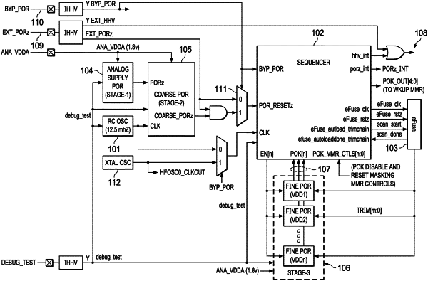
a power on reset (PoR) stage comprising:
a set of voltage level detectors;
a first input terminal coupled to the set of voltage level detectors, the first input terminal configured to receive first, second and third supply voltages;
a second input terminal coupled to the set of voltage level detectors, the second input terminal configured to receive trim values;
a first output terminal coupled to the set of voltage level detectors to provide a first power OK signal based on a first comparison of the first supply voltage to a select one of the trim values;
a second output terminal coupled to the set of voltage level detectors to provide a second power OK signal based on a second comparison of the second supply voltage to a select one of the trim values; and
a third output terminal coupled to the set of voltage level detectors to provide a third power OK signal based on a third comparison of the third supply voltage to a select one of the trim values; and
a sequencer comprising:
first AND logic comprising:
a first input terminal coupled to the first output terminal of the PoR stage to receive the first power OK signal;
a second input terminal to receive a first mask signal; and
an output terminal;
second AND logic comprising:
a first input terminal coupled to the second output terminal of the PoR stage to receive the second power OK signal;
a second input terminal to receive a second mask signal; and
an output terminal;
third AND logic comprising:
a first input terminal coupled to the third output terminal of the PoR stage to receive the third power OK signal;
a second input terminal to receive a third mask signal; and
an output terminal;
OR logic comprising:
a first input terminal coupled to the output terminal of the first AND logic;
a second input terminal coupled to the output terminal of the second AND logic;
a third input terminal coupled to the output terminal of the third AND logic; and
an output terminal, wherein:
the sequencer is configured to de-assert a reset signal based on each of the first power OK signal, the second power OK signal, and the third power OK signal; and
the first mask signal, the second mask signal, and the third mask signal are configured to inhibit a response of the reset signal during an update of the trim value.
|