| CPC H03F 1/223 (2013.01) [G01R 31/2834 (2013.01); H03F 3/195 (2013.01); H03F 3/245 (2013.01); H03F 3/72 (2013.01); H03F 2200/261 (2013.01); H03F 2200/294 (2013.01); H03F 2200/451 (2013.01)] | 20 Claims |

|
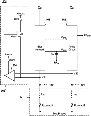
1. An integrated circuit including:
(a) an active circuit including a first ground connection;
(b) a bias network coupled to the active circuit and including a second ground connection, the bias network configured to provide a calibrated bias voltage to the active circuit corresponding to a specified current for the active circuit; and
(c) a calibration switch coupled between the first ground connection and the second ground connection, the calibration switch configured to be closed during calibration of the active circuit and open after completion of calibration of the active circuit.
|