| CPC H01S 5/4031 (2013.01) [H01S 5/0234 (2021.01); H01S 5/02461 (2013.01); H01S 5/02469 (2013.01); H01S 5/0421 (2013.01); H01S 5/32341 (2013.01); H01S 5/04254 (2019.08); H01S 5/22 (2013.01)] | 12 Claims |

|
1. An edge-emitting laser bar comprising:
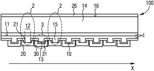
an AlInGaN-based semiconductor layer sequence having a contact side and an active layer configured to generate laser radiation;
a plurality of individual emitters arranged next to each other and spaced apart from one another in a lateral transverse direction, each emitter configured to emit laser radiation; and
a plurality of contact elements arranged next to each other and spaced apart from one another in the lateral transverse direction on the contact side for making electrical contact with the individual emitters, each contact element being assigned to an individual emitter,
wherein each contact element is electrically conductively coupled to the semiconductor layer sequence via a contiguous contact region of the contact side so that a current flow between the semiconductor layer sequence and the contact element is possible via the contact region,
wherein the laser bar has a thermal decoupling structure in a region between two adjacent individual emitters, the thermal decoupling structure being configured to counteract a heat exchange between the two adjacent individual emitters,
wherein the decoupling structure comprises an electrically conductive cooling element located on the contact side and completely covering a contiguous cooling region of the contact side,
wherein the cooling element is electrically isolated from the semiconductor layer sequence along the cooling region and thermally coupled to the semiconductor layer sequence along the cooling region,
wherein the cooling region has a width, measured along the lateral transverse direction, which is at least half a width of an adjacent contact region,
wherein all contact elements are arranged equidistantly to each other,
wherein one or more cooling elements are arranged in the region between each two individual emitters and are in each case elements which are different from the contact elements,
wherein the cooling elements in the cooling region are spaced from the contact side of the semiconductor layer sequence by a separating layer, and wherein the separating layer comprises one of the following materials: SiC, DLC or AIN.
|