| CPC H01Q 21/065 (2013.01) [H01Q 1/48 (2013.01); H01Q 1/523 (2013.01); H01Q 9/0421 (2013.01)] | 5 Claims |

|
1. An antenna array comprising:
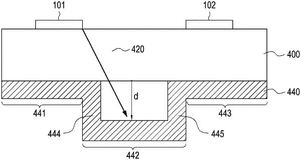
a dielectric;
a first patch antenna disposed on a first area of the dielectric;
a second patch antenna disposed on a second area of the dielectric; and
a ground layer disposed on a bottom of the dielectric, wherein the ground layer includes a first sub-ground layer contacting the first area of the dielectric, a third sub-ground layer contacting the second area of the dielectric, and a second sub-ground layer distanced from the bottom of the dielectric and disposed between the first sub-ground layer and the third sub-ground layer, and
wherein the ground layer includes a first connection portion connecting between the first sub-ground layer and the second sub-ground layer, and a second connection portion connecting between the second sub-ground layer and the third sub-ground layer.
|