| CPC H01L 33/387 (2013.01) [H01L 25/167 (2013.01); H01L 33/382 (2013.01); H01L 33/385 (2013.01); H01L 33/44 (2013.01); H01L 33/14 (2013.01); H01L 33/32 (2013.01)] | 21 Claims |

|
1. A display device, comprising:
a substrate;
a driving device disposed on substrate;
a light-emitting device electrically connected to the driving device, comprising first and second areas;
a pixel electrode connected to the light-emitting device and the driving device; and
a common electrode connected to the light-emitting device and a common power line,
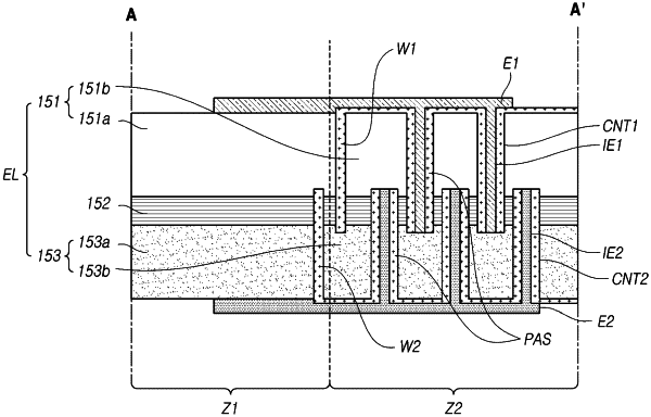
wherein the light-emitting device comprises:
a p-type semiconductor layer comprising a first p-type semiconductor layer in the first area and a second p-type semiconductor layer in the second area;
an n-type semiconductor layer comprising a first n-type semiconductor layer in the first area and a second n-type semiconductor layer in the second area;
an active layer between the p-type semiconductor layer and the n-type semiconductor layer;
a first electrode on the p-type semiconductor layer and having a first inner electrode connected to the second n-type semiconductor layer in the second area;
a second electrode on the n-type semiconductor layer and having a second inner electrode connected to the second p-type semiconductor layer in the second area;
a first wall by which the first and second p-type semiconductor layers are divided from each other; and
a second wall by which the first and second n-type semiconductor layers are divided from each other,
wherein the first p-type semiconductor layer and the first n-type semiconductor layer are disposed in the first area configured to emit light when a forward bias is applied to the first electrode connected to the first p-type semiconductor layer and the second electrode connected to the first n-type semiconductor layer, and
wherein the second p-type semiconductor layer and the second n-type semiconductor layer are disposed in the second area configured to emit light when a reverse bias is applied to the first electrode connected to the second n-type semiconductor layer and the second electrode connected to the second p-type semiconductor layer.
|