| CPC H01L 33/005 (2013.01) [H01L 27/156 (2013.01); H01L 33/502 (2013.01); H01L 2933/0041 (2013.01); H01L 2933/0058 (2013.01)] | 18 Claims |

|
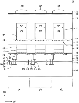
1. A display device comprising:
a support substrate;
a first light-emitting area on the support substrate, the first light-emitting area comprising:
a first semiconductor layer provided on the support substrate;
an active layer provided on the first semiconductor layer of the first light-emitting area;
a second semiconductor layer provided on the active layer of the first light-emitting area;
a first contact electrically connecting the support substrate and the first semiconductor layer of the first light-emitting area;
a first common electrode provided on the second semiconductor layer of the first light-emitting area, the first common electrode being configured to be electrically connected to the second semiconductor layer of the first light-emitting area; and
a first color adjustment pattern formed on the first light-emitting area,
wherein the active layer is provided on a first surface of the second semiconductor layer and the first common electrode is provided on a second surface of the second semiconductor layer opposite to the first surface of the second semiconductor layer.
|