| CPC H01L 29/8725 (2013.01) [H01L 29/24 (2013.01); H01L 29/47 (2013.01); H01L 29/7802 (2013.01)] | 3 Claims |

|
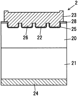
2. A Schottky barrier diode, comprising:
a first semiconductor layer that comprises a Ga2O3-based single crystal and has a trench opening on one surface;
a second semiconductor layer that comprises a Ga2O3-based single crystal and is stacked on a surface of the first semiconductor layer on which the trench is not open;
an insulating film covering an inner surface of the trench;
a trench MOS barrier buried in the trench so as to be covered with the insulating film;
an anode electrode that forms a Schottky junction with the first semiconductor layer, is in contact with the trench MOS barrier and is configured so that a portion in contact with the first semiconductor layer comprises Mo or W; and
a cathode electrode connected to the second semiconductor layer,
wherein the first semiconductor layer is configured such that a turn-on voltage thereof is not less than 0.4 V and not more than 0.6 V.
|