| CPC H01L 29/872 (2013.01) [H01L 21/761 (2013.01); H01L 29/0646 (2013.01); H01L 29/0649 (2013.01); H01L 29/2003 (2013.01); H01L 29/205 (2013.01); H01L 29/402 (2013.01); H01L 29/404 (2013.01); H01L 29/66143 (2013.01); H01L 29/66212 (2013.01); H01L 29/7786 (2013.01); H01L 29/861 (2013.01); H02M 7/003 (2013.01)] | 26 Claims |

|
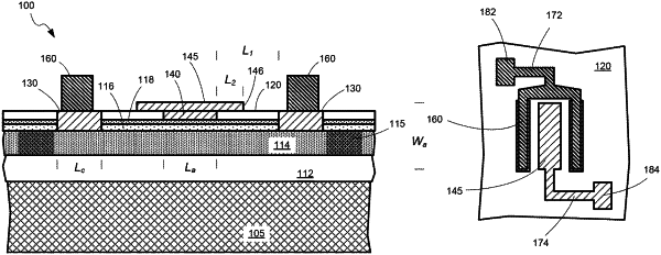
1. A Schottky diode comprising:
a conduction layer;
a first layer comprising a first semiconductor material over the conduction layer;
a second layer comprising a second semiconductor material over the first layer, the first semiconductor material being different than the second semiconductor material;
a first cathode and a second cathode, spaced apart and in electrical contact with the conduction layer, the first cathode and the second cathode being electrically connected to each other as a cathode of the Schottky diode; and
an anode over the second layer between the first cathode and the second cathode.
|