| CPC H01L 29/8083 (2013.01) [H01L 29/0843 (2013.01); H01L 29/1058 (2013.01); H01L 29/1095 (2013.01); H01L 29/407 (2013.01); H01L 29/42316 (2013.01)] | 4 Claims |

|
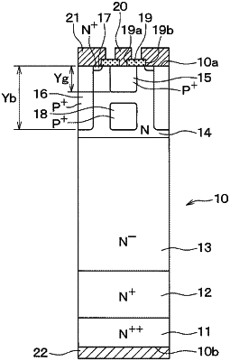
1. A semiconductor device comprising:
a drift layer of a first conductivity type;
a channel layer of the first conductivity type disposed on a surface of the drift layer;
a source layer of the first conductivity type having a higher impurity concentration than the channel layer, the source layer disposed on a surface layer portion of the channel layer;
a gate layer of a second conductivity type disposed at the channel layer and arranged to be deeper than the source layer;
a body layer of the second conductivity type disposed at the channel layer, the body layer arranged to be deeper than the source layer while being separated from the gate layer;
a shield layer disposed at a part of the channel layer located between the gate layer and the drift layer, the shield layer facing the gate layer while being separated from the gate layer, the shield layer maintained at a potential different from a potential of the gate layer; and
a drain layer disposed at a side opposite to the channel layer so that the drift layer is sandwiched between the drain layer and the channel layer,
wherein a depth ratio of a depth of the gate layer to a depth of the body layer is equal to or smaller than 0.45,
wherein the semiconductor device has a junction-type field effect transistor,
wherein the drift layer the channel layer are stacked in a stacking direction,
wherein the gate layer is extended in a direction being a longitudinal direction, as viewed in the stacking direction,
wherein the body layer is arranged along the stacking direction,
wherein the longitudinal direction is normal to a cross sectional view of the semiconductor device,
wherein, in the cross sectional view, the channel layer extends from a bottom of the source layer to the surface of the drift layer in the stacking direction and
wherein, in the cross sectional view, the shield layer is disposed at a location between a center of the gate layer in a width direction, which is perpendicular to the stacking direction and the longitudinal direction, and the drift layer.
|