| CPC H01L 29/7805 (2013.01) [H01L 21/0465 (2013.01); H01L 29/063 (2013.01); H01L 29/1095 (2013.01); H01L 29/1608 (2013.01); H01L 29/66068 (2013.01)] | 20 Claims |

|
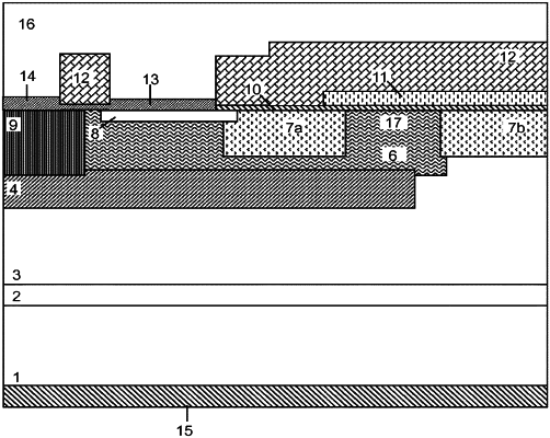
1. A method of manufacturing a MOSFET device in SiC, the method comprising:
forming a drift layer in contact with a substrate, a buried grid in contact with the drift layer, and a well above the buried grid;
defining a self-aligned lateral MOS channel for a MOSFET circuit by simultaneously forming an access region and a JFET region within the well, the access and JFET regions being laterally self-aligned and having an intermediate part of the well therebetween;
forming a source in contact with the well and the access region;
forming a body for a body diode circuit in contact with the well and the buried grid;
forming a source contact and a body diode contact, the source contact for the MOSFET circuit being in contact with the source, the body diode contact for the body diode circuit being in contact with the body;
forming an insulating gate oxide on a portion of the source, the access region, the intermediate part of the well, and the JFET region;
forming a gate contact on the insulating gate oxide, and forming an isolation layer on the gate contact; and
forming a drain contact in contact with the substrate.
|