| CPC H01L 29/7786 (2013.01) [H01L 21/8252 (2013.01); H01L 27/0605 (2013.01); H01L 27/085 (2013.01); H01L 27/088 (2013.01); H01L 29/66462 (2013.01); H01L 29/7787 (2013.01)] | 13 Claims |

|
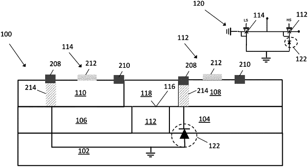
1. A semiconductor device, comprising:
a base substrate of type IV semiconductor material comprising a rear surface and an upper surface opposite the rear surface;
first and second device areas that are electrically isolated from one another and each extend to the upper surface;
a first region of type III-V semiconductor material formed on the base substrate over the first device area;
a second region of type III-V semiconductor material formed on the base substrate over the second device area, the second region of type III-V semiconductor material being laterally electrically insulated from the first region of type III-V semiconductor material;
a first high-electron mobility transistor integrally formed in the first region of type III-V semiconductor material; and
a second high-electron mobility transistor integrally formed in the second region of type III-V semiconductor material,
wherein the first and second high-electron mobility transistors each comprise source and drain terminals and are each configured to control a conductive connection between the respective source and drain terminals; and
wherein the first and second high-electron mobility transistors are connected in series with the source terminal of the first high-electron mobility transistor connected to the drain terminal of the second high-electron mobility transistor,
wherein the source terminal of the first high-electron mobility transistor is electrically connected to the first device area, and
wherein the first device area is electrically isolated from a subjacent region of the base substrate by a first two-way voltage blocking device.
|